Erich Focht
Introduction
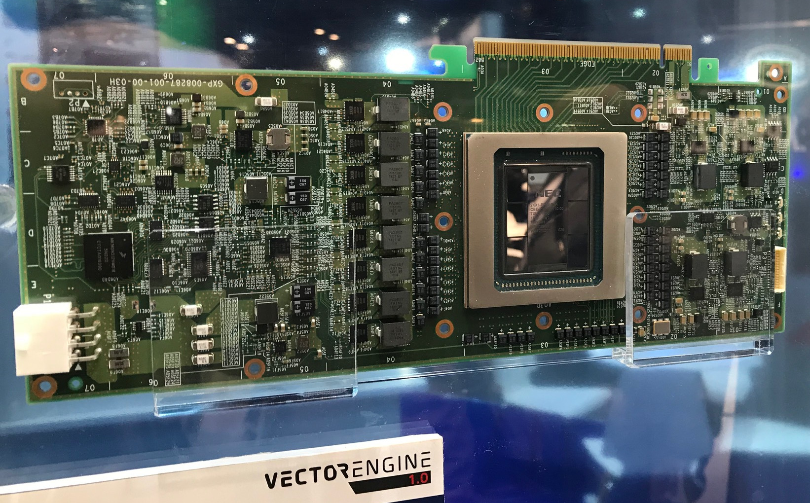
The SX-Aurora TSUBASA is a vector processor card in PCIe form factor. It was built in the tradition of the NEC SX-series architecture but represents a radical change in the system design. While the old SX vector supercomputers were conceptually close to mainframes with proprietary hardware, very specialized interconnect network, proprietary SuperUX operating system, the SX-Aurora is a rather small card, built into a x86 Linux server or PC, using Infiniband interconnects for communication. The vector engine can be used either as a vector computer or as an accelerator for hybrid x86-VE codes.
Processor Architecture
The vector engine is a processor with only 8 powerfull cores, sharing a 16MB cache (LLC = last level cache) and connected to 6 HBM2 modules through the Silicon interposer (Chip-on-Wafer-on-Substrate technology). It has currently the largest memory bandwidth among all current processors and accelerators: 1.22 TB/s.
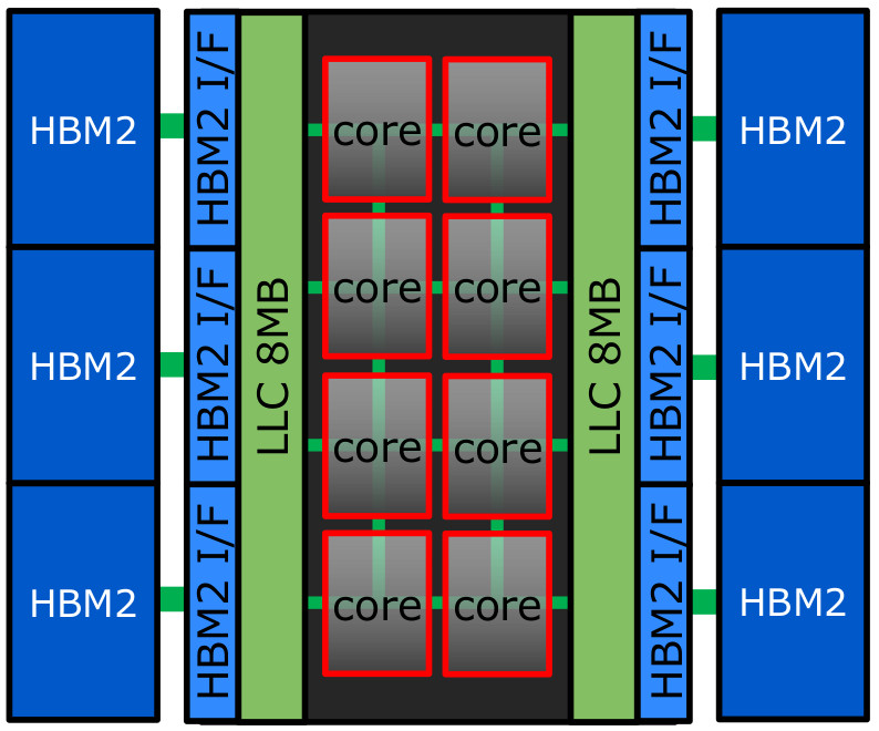
The peak bandwidth per core is 400GB/s and the maximum bandwidth available from LLC is 3TB/s.
The VE is manufactured in a 16nm FinFET process and available in three variants listed in the table below. Variant 10A is only sold in the direct liquid cooled version.
| VE SKUs | 10A | 10B | 10C |
|---|---|---|---|
| Clock Speed | 1.6GHz | 1.4GHz | 1.4GHz |
| Core DP GFLOPS | 307.2 | 268.8 | 268.8 |
| CPU DP TFLOPS | 2.45 | 2.15 | 2.15 |
| CPU SP TFLOPS | 4.9 | 4.3 | 4.3 |
| Memory bandwidth | 1.22TB/s | 1.22TB/s | 0.76TB/s |
| Memory capacity | 48GB | 48GB | 24GB |
VE Core, Registers, Functional Units
Each core of the VE has a fully featured Scalar Processing Unit (SPU) with L1 and L2 caches (32kB+32kB, 256kB) and 64 scalar registers.
The Vector Processing Unit (VPU) components are:
- 64 vector registers of 256 * 64 bits = 16 kilobits, each. They are implemented as mixed SIMD (32 * 64 bits wide) + pipelined units.
- 3 vector fused multiply and add units (FMA) able of delivering 3 * 32 * 2 = 192 double precision results per clock cycle.
- 2 vector arithmetic logical units (ALU) for fixed point arithmetic processing.
- one dedicated full precision divide unit.
Instruction processing is out-of-order for both SPU and VPU.
The combination of SIMD and pipelining allows a very efficient use of the functional unit stages and results in rather low power consumption. For example the 10B model’s peak TDP is 300W, it is said to spend 250W during the HPL benchark and less than 150W during HPCG.
The cores have address translation buffers (AKA TLBs) for virtual memory addressing and DMA engines for asyncronous memory movement eg. over the PCIe bus.
While memory addressing is done in pages and processes use a virtual address space, the extremely high memory bandwidth during vector operations does not allow precise exceptions. Basically this means that vector operations can’t recover from page faults, therefore programs are executed in a “real memory mode”, where all memory that might be touched by the CPU must be available while the process is running.
VE Instruction Set Architecture
The SPU’s instruction set is that of a rather complete RISC microprocessor. The scalar instructions operate on/with the 64 scalar registers and system registers and can be grouped into following classes:
- Transfer instructions
- Fixed-Point Arithmetic Operations
- Logical Arithmetic Operations
- Shift Instructions
- Floating-Point Arithmetic Operations
- Branch Instructions
- Control Instructions
- Host Memory Access Instructions
Vector instructions are operating on/with the 64 vector registers and 16 vector mask registers. The main difference to the widely spread SIMD instructions nowadays called “vector instructions” is that vector instructions are controlled by a vector length register. This is neither a mask nor does it limit configure SIMD units. It contains a number between 1 and 256 which controls how many elements of the vector registers will be processed. It can be set any time!
Vector instruction classes are:
- Transfer instructions
- Fixed-Point Arithmetic Operations
- Logical Arithmetic Operations
- Shift Instructions
- Floating-Point Arithmetic
- Vector Mask Arithmetic Instructions
- Recursive Relations Instructions
- Gather/Scatter Instructions
- Vector Mask Register Instructions
- Vector Control Instructions
- Vector 2D Load/Store Instructions
A glimpse at system software and usage models
The VE looks very much like an accelerator card, a GPGPU and alike, but can be used like a normal vector computer: programming is in high level languages: C, C++, Fortran, parallelization is done with OpenMP and MPI, and native VE programs behave as if they’d see a rather standard Linux environment. Native VE applications can call almost any Linux system call, it will mostly be forwarded and handled on the vector host (VH) side. Systems built with VEs can be linked together with Infiniband and native VE programs can communicate with each other in PeerDirect style without involving the host.
Of course, the accelerator card can also be used as an … accelerator! The low level API for hybrid OpenCL or CUDA alike VE programming is called VEO, see for example veoffload at github.com or py-veo at github.com.
Native VE programs can also use the x86 VH as an accelerator with the VHcall reverse offloading mechanisms.
Finally, some day we will be able to use hybrid MPI for truly hybrid codes :-)